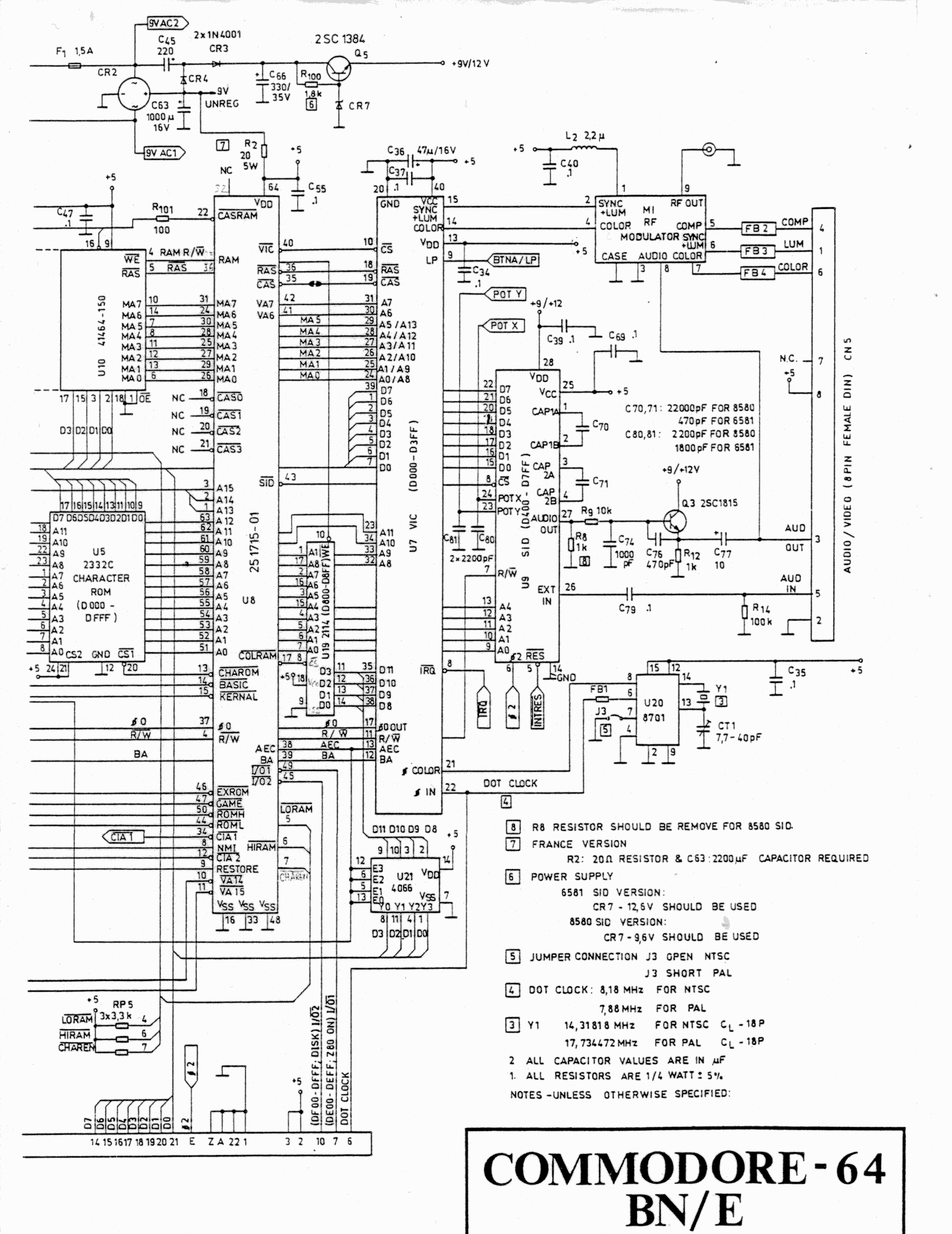
251715-01 / 252535-01 memory controller (C64C) pinout
DIP-64. PLA, DRAM address multiplexer and chip selects in one chip (C64C short board)
Replaces the 82S100 PLA and its helpers on the 250469 short board. It makes the ROM, I/O and cartridge selects, the chip selects for the VIC-II, SID and both CIAs, and the multiplexed DRAM address MA0-MA7 with gated /CAS. Rev A boards fit the 251715-01 with a separate 2114 color RAM at U19 (pin 17 /COLRAM selects it). Rev B boards fit the 252535-01, which holds the color RAM itself: pins 18-21 carry its four data bits, and pin 17 has no RAM to select. Do not swap one type for the other without checking the board. The package is a shrink DIP: 64 pins in about the length of the 40-pin VIC-II (1.78 mm pitch on the board photos). A dead one gives a black screen, as a dead PLA does.
Open the interactive 251715 pinoutPins
| Pin | Name | Type | Signal |
|---|---|---|---|
| 1 | A13 | addr | Address bit 13. |
| 2 | A14 | addr | Address bit 14. |
| 3 | A15 | addr | Address bit 15. |
| 4 | R/W | ctrl | Read/write from the CPU. HIGH = read, LOW = write. |
| 5 | LORAM | ctrl | CPU port bit 0: BASIC ROM banking. |
| 6 | HIRAM | ctrl | CPU port bit 1: KERNAL ROM banking. |
| 7 | CHAREN | ctrl | CPU port bit 2: character ROM or I/O at $D000. |
| 8 | NMI | ctrl | NMI line to the CPU (schematic name NMI). Pin 9 takes the RESTORE key. UNVERIFIED |
| 9 | RESTORE | ctrl | RESTORE key input. UNVERIFIED |
| 10 | /VA14 | ctrl | VIC-II bank select bit 14, from CIA2 port A. |
| 11 | /VA15 | ctrl | VIC-II bank select bit 15, from CIA2 port A. |
| 12 | /CIA2 | ctrl | CIA2 chip select ($DD00-$DDFF). |
| 13 | /CHAROM | ctrl | Character ROM select (U5). |
| 14 | /BASIC | ctrl | BASIC ROM select. Drawn on the rev A schematic; the rev B schematic draws a wire only at pin 15 for the one BASIC/KERNAL ROM. UNVERIFIED |
| 15 | /KERNAL | ctrl | KERNAL ROM select (labeled /BASIC and /KERNAL on the rev B schematic). |
| 16 | VSS | ground | 0 V. |
| 17 | /COLRAM | ctrl | 251715: color RAM select to the 2114 at U19 (pin 8). 252535: no external color RAM; the rev B schematic draws this pin to +5 V. UNVERIFIED |
| 18 | CAS0 / D1 | data | 251715: CAS0, not connected on the board. 252535: color RAM data bit D1, on the VIC-II color data lines D8-D11. UNVERIFIED |
| 19 | CAS1 / D2 | data | 251715: CAS1, not connected on the board. 252535: color RAM data bit D2. UNVERIFIED |
| 20 | CAS2 / D3 | data | 251715: CAS2, not connected on the board. 252535: color RAM data bit D3. UNVERIFIED |
| 21 | CAS3 / D4 | data | 251715: CAS3, not connected on the board. 252535: color RAM data bit D4. UNVERIFIED |
| 22 | /CASRAM | ctrl | Gated /CAS to the DRAMs (through R101). |
| 23 | RAM R/W | ctrl | Write enable to the DRAMs (/WE). |
| 24 | MA6 | addr | Multiplexed DRAM address bit 6. |
| 25 | MA3 | addr | Multiplexed DRAM address bit 3. |
| 26 | MA0 | addr | Multiplexed DRAM address bit 0. |
| 27 | MA2 | addr | Multiplexed DRAM address bit 2. |
| 28 | MA4 | addr | Multiplexed DRAM address bit 4. |
| 29 | MA1 | addr | Multiplexed DRAM address bit 1. |
| 30 | MA5 | addr | Multiplexed DRAM address bit 5. |
| 31 | MA7 | addr | Multiplexed DRAM address bit 7. |
| 32 | NC | nc | No connection. |
| 33 | VSS | ground | 0 V. |
| 34 | /CIA1 | ctrl | CIA1 chip select ($DC00-$DCFF). |
| 35 | /CAS | ctrl | Column address strobe from the VIC-II. |
| 36 | /RAS | ctrl | Row address strobe from the VIC-II. |
| 37 | Φ0 | clock | System clock Φ0 from the VIC-II. |
| 38 | AEC | ctrl | Address Enable Control from the VIC-II. |
| 39 | BA | ctrl | Bus Available from the VIC-II. |
| 40 | /VIC | ctrl | VIC-II chip select ($D000-$D3FF). |
| 41 | VA6 | addr | VIC-II address bit 6 (for the DRAM address multiplexer). |
| 42 | VA7 | addr | VIC-II address bit 7. |
| 43 | /SID | ctrl | SID chip select ($D400-$D7FF). |
| 44 | /ROML | ctrl | Cartridge low ROM select (expansion port). |
| 45 | /IO2 | ctrl | I/O 2 select ($DF00-$DFFF, expansion port). |
| 46 | /EXROM | ctrl | EXROM line from the expansion port. |
| 47 | /GAME | ctrl | GAME line from the expansion port. |
| 48 | VSS | ground | 0 V. |
| 49 | /IO1 | ctrl | I/O 1 select ($DE00-$DEFF, expansion port). |
| 50 | /ROMH | ctrl | Cartridge high ROM select (expansion port). |
| 51 | A0 | addr | Address bit 0. |
| 52 | A1 | addr | Address bit 1. |
| 53 | A2 | addr | Address bit 2. |
| 54 | A3 | addr | Address bit 3. |
| 55 | A4 | addr | Address bit 4. |
| 56 | A5 | addr | Address bit 5. |
| 57 | A6 | addr | Address bit 6. |
| 58 | A7 | addr | Address bit 7. |
| 59 | A8 | addr | Address bit 8. |
| 60 | A9 | addr | Address bit 9. |
| 61 | A10 | addr | Address bit 10. |
| 62 | A11 | addr | Address bit 11. |
| 63 | A12 | addr | Address bit 12. |
| 64 | VDD | power | +5 V supply. |
Fitted in
- Commodore 64 U8 (250469 boards: 251715-01 on rev A, 252535-01 on rev B)
Sources
- Commodore schematic 252312 rev A (250469 rev A), right half: U8 251715-01 with pin numbers
- Commodore schematic 252311 rev B (corrected, combined): U8 252535-01 with pin numbers
- C64/C64C Service Manual 314001-03, parts list 250469-01: U8 Memory Controller 251715-01, PDF p. 50
- 250469 rev A schematic, drawn by Falk Brunner (PDF), sheet 2: U8 "SUPER PLA" 251715-01