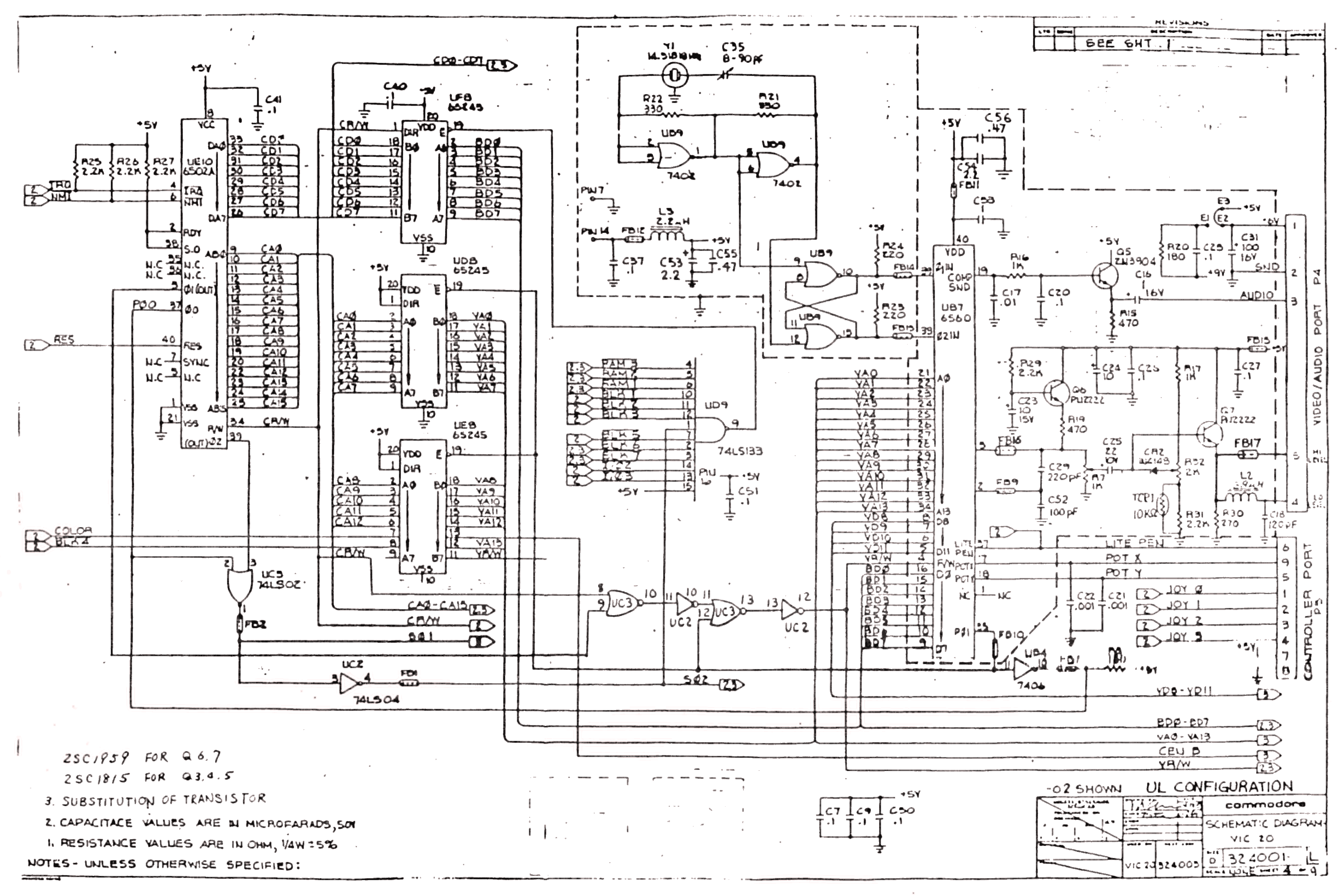
6560 / 6561 VIC-I pinout
DIP-40. Video, sound, paddles, light pen, CPU clock
The VIC-20 video and sound chip at $9000-$900F. 6560 is NTSC, 6561 is PAL. Runs from +5 V only (the VIC-20 has no +12 V rail). Makes the color, three tones and noise, and reads the paddles. A failure gives no or garbled picture and no sound.
Open the interactive VIC pinoutPins
| Pin | Name | Type | Signal |
|---|---|---|---|
| 1 | NC | nc | No connection. |
| 2 | COMP COLOR | video | Composite color (chroma) output to the video circuit. |
| 3 | SYNC & LUM | video | Sync and luminance output to the video circuit. |
| 4 | R/W | ctrl | Read/write from the CPU. |
| 5 | DB11 | data | Data bit 11. DB8-DB11 only read the color nybble from color RAM; DB0-DB7 are the bidirectional CPU bus. |
| 6 | DB10 | data | Data bit 10, color nybble from color RAM (input only). |
| 7 | DB9 | data | Data bit 9, color nybble from color RAM (input only). |
| 8 | DB8 | data | Data bit 8, color nybble from color RAM (input only). |
| 9 | D7 | data | Data bus bit 7. |
| 10 | D6 | data | Data bus bit 6. |
| 11 | D5 | data | Data bus bit 5. |
| 12 | D4 | data | Data bus bit 4. |
| 13 | D3 | data | Data bus bit 3. |
| 14 | D2 | data | Data bus bit 2. |
| 15 | D1 | data | Data bus bit 1. |
| 16 | D0 | data | Data bus bit 0. |
| 17 | POT X | audio | Paddle A/D input X (control port pin 9). |
| 18 | POT Y | audio | Paddle A/D input Y (control port pin 5). |
| 19 | COMP SND | audio | Composite sound output: three tones and noise. |
| 20 | GND | ground | 0 V. |
| 21 | A0 | addr | Address bit 0. Input while PΦ2 is high (register select within $9000-$900F); output while PΦ1 is high, when the VIC fetches screen and character data. |
| 22 | A1 | addr | Address bit 1. |
| 23 | A2 | addr | Address bit 2. |
| 24 | A3 | addr | Address bit 3. |
| 25 | A4 | addr | Address bit 4. |
| 26 | A5 | addr | Address bit 5. |
| 27 | A6 | addr | Address bit 6. |
| 28 | A7 | addr | Address bit 7. |
| 29 | A8 | addr | Address bit 8. |
| 30 | A9 | addr | Address bit 9. |
| 31 | A10 | addr | Address bit 10. |
| 32 | A11 | addr | Address bit 11. |
| 33 | A12 | addr | Address bit 12. |
| 34 | A13 | addr | Address bit 13. |
| 35 | PΦ1 | clock | Processor clock phase 1 output. |
| 36 | PΦ2 | clock | Processor clock phase 2 output. |
| 37 | OPTION | ctrl | Data sheet name OPTION. The VIC-20 schematic wires it as the light pen input (control port pin 6). |
| 38 | Φ2 IN | clock | Phase 2 clock input. |
| 39 | Φ1 IN | clock | Phase 1 clock input. |
| 40 | VDD | power | +5 V supply (VIC-20 is +5 V only). |
Fitted in
- VIC-20 UB7
Sources
- MOS 6560/6561 Video Interface Chip data sheet, p. 1 pin configuration and scan 6560-09 pin signal description (address bus bidirectional; DB8-DB11 color data only) (GIF scans)
- VIC-20 Programmer's Reference Guide, 6560 pin configuration, p. 212
- VIC-20 schematic 324001 sheet 1 (pin 37 used as light pen)