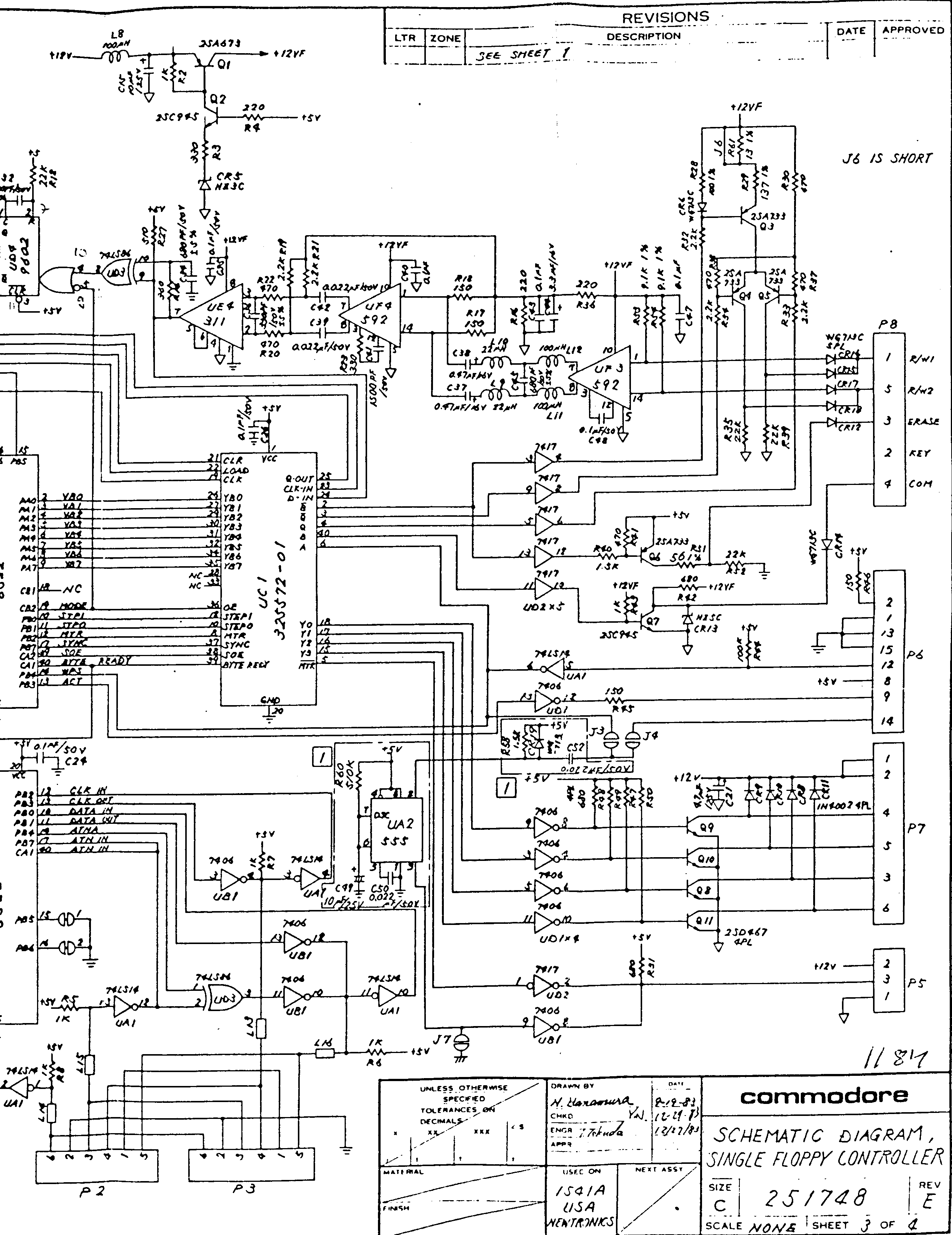
325572-01 (64H105) 40-pin gate array pinout
DIP-40. 1541 short board read/write logic: GCR shift register, byte-ready, sync detect, stepper phases, spindle motor driver
Replaces the long board's discrete read/write and stepper logic (service manual PDF p. 13). Parallel data YB0-YB7 to and from VIA UC2 port A, BYTE READY on pin 39, SYNC on pin 37, stepper phases Y0-Y3 from STEP0/STEP1, and the inverted /MTR on pin 5 to the spindle motor board. Pins 7, 9, 11, 13 and 14 are not drawn on schematic 251748. Ray Carlsen found one bad 325572 in about 40 repaired 1541s: rare.
Open the interactive 325572 pinoutPins
| Pin | Name | Type | Signal |
|---|---|---|---|
| 1 | VCC | power | +5 V supply. |
| 2 | /B | ctrl | Write enable, inverted. LOW during a write turns on the erase coil driver (Q3, Q6). |
| 3 | /Q | io | Write data, inverted. LOW drives current through R/W coil 2. |
| 4 | Q | io | Write data. LOW drives current through R/W coil 1. |
| 5 | /MTR | ctrl | Spindle motor on, inverted, to the 7417 driver (UD2 on the short board, UG4 on the long board) and the motor control board. |
| 6 | A | io | Labeled A on schematic 251748; drawn in the write circuit. Function not described in the service manual. UNVERIFIED |
| 7 | NC | nc | Not drawn on schematic 251748; no signal listed in pla.txt. UNVERIFIED |
| 8 | MTR | ctrl | Spindle motor on, from VIA UC2 PB2. |
| 9 | NC | nc | Not drawn on schematic 251748; no signal listed in pla.txt. UNVERIFIED |
| 10 | STEP0 | ctrl | Stepper count bit 0, from VIA UC2 port B. |
| 11 | NC | nc | Not drawn on schematic 251748; no signal listed in pla.txt. UNVERIFIED |
| 12 | STEP1 | ctrl | Stepper count bit 1, from VIA UC2 port B. |
| 13 | NC | nc | Not drawn on schematic 251748; no signal listed in pla.txt. UNVERIFIED |
| 14 | NC | nc | Not drawn on schematic 251748; no signal listed in pla.txt. UNVERIFIED |
| 15 | Y3 | ctrl | Stepper phase 3, to the 7406 phase drivers. |
| 16 | Y2 | ctrl | Stepper phase 2. |
| 17 | Y1 | ctrl | Stepper phase 1. |
| 18 | Y0 | ctrl | Stepper phase 0. |
| 19 | CLK | clock | Bit clock from the density counter (74LS193). UNVERIFIED |
| 20 | GND | ground | Ground. |
| 21 | CLR | ctrl | Clear from the read circuit (a flux change was read). UNVERIFIED |
| 22 | LOAD | ctrl | Load strobe from the density counter. UNVERIFIED |
| 23 | CLK-IN | clock | Clock in (labeled CLK-IN on schematic 251748). |
| 24 | D-IN | io | Serial read data in from the read amplifier (service manual PDF p. 13). |
| 25 | Q-OUT | io | Output labeled Q-OUT on schematic 251748. |
| 26 | YB0 | data | Parallel data bit 0, to VIA UC2 PA0. |
| 27 | YB1 | data | Parallel data bit 1, to VIA UC2 PA1. |
| 28 | NC | nc | No connection (NC on schematic 251748). |
| 29 | YB2 | data | Parallel data bit 2, to VIA UC2 PA2. |
| 30 | YB3 | data | Parallel data bit 3, to VIA UC2 PA3. |
| 31 | YB4 | data | Parallel data bit 4, to VIA UC2 PA4. |
| 32 | YB5 | data | Parallel data bit 5, to VIA UC2 PA5. |
| 33 | NC | nc | No connection (NC on schematic 251748). |
| 34 | YB6 | data | Parallel data bit 6, to VIA UC2 PA6. |
| 35 | YB7 | data | Parallel data bit 7, to VIA UC2 PA7. |
| 36 | OE | ctrl | Read/write mode, from VIA UC2 CB2 (MODE). |
| 37 | SYNC | ctrl | Sync detect to VIA UC2 PB7: goes LOW while a sync mark (all ones) is read. |
| 38 | SOE | ctrl | Byte-ready enable, from VIA UC2 CA2. |
| 39 | /BYTE READY | ctrl | Byte ready: LOW when a byte is latched on YB0-YB7. Goes to VIA UC2 CA1 and the 6502 SO pin. |
| 40 | B | ctrl | Write enable. HIGH during a write (service manual PDF p. 16). |
Fitted in
- Commodore 1541 disk drive UC1 (short boards 1540048, 250442, 250446; not on the long board, which does this in TTL)